TORYZA EL PROCESS,
 UBM formation for power semiconductors
Electroless plating process and plating equipment
TORYZA EL PROCESS, TORYZA EL SYSTEM
Power semiconductors refer to a category of semiconductors responsible for regulating and converting power, often referred to as power devices.
In analogy to the human body, where Large Scale Integrated Circuits (LSI) such as CPUs and GPUs serve as the "brain", power semiconductors can be compared to the "muscle" or "heart". They play a critical role in controlling the motors in EVs and the sensors in cameras and other applications.
With their ability to regulate voltage and power and minimize electrical losses, power semiconductors are widely used in various technologies such as smartphones, PCs, air conditioners, automobiles, and industrial equipment. The power semiconductor market is expected to grow steadily.
Role required for UBM (Under Barrier Metal)
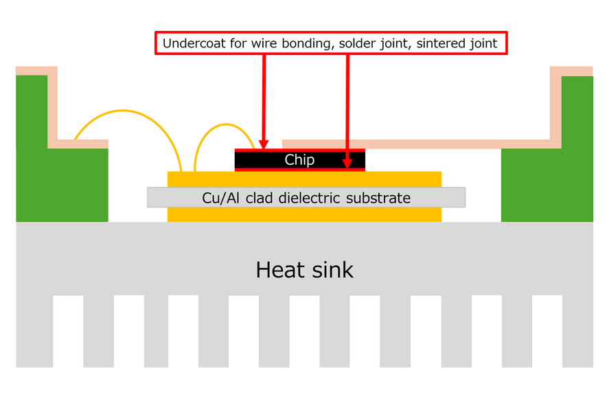
Power modules, which regulate and transform electrical power, embody semiconductor chips in them.
Electroless plating, referred to as UBM (Under Barrier Metal), is employed when bonding aluminum electrodes on chips to package terminals or to copper/aluminum clad dielectric substrates using wire bonding or lead-containing solder.
Recently, in an effort to eliminate harmful substances from bonding materials, sintered bonding with metal nanoparticles, such as copper and silver, has gained attention as an alternative to lead-containing solder.
UBM is one of the key steps in the semiconductor manufacturing process and plays the following roles.
- Wiring connections: Carry electrical signals on a chip to external wiring or other chips.
- Reliability improvement: Improve reliability between interconnects/pads.
- Provide conductivity: Provide conductivity between interconnects and pads.
- Barrier function: Act as a barrier between interconnects and pads, preventing unintended metal diffusion between interconnects or electrodes and pads.
- Heat Resistance: Prevent degradation of physical properties due to heat generation.
From the above, UBM plays an important role in improving reliability and performance as a part of the semiconductor manufacturing process.
Electroless plating process to enhance heat resistance of power semiconductor components
TORYZA EL PROCESS
Power semiconductors can handle high voltages and high currents. However, the flow of high voltages and currents in their circuits generates significant heat.
Inadequate thermal management can cause surrounding components to melt, resulting in device malfunctions that damage the safety, performance, and reliability of electronic appliances containing these semiconductor devices.
To prevent such failures, we need to provide effective heat radiation and heat release methods for these power semiconductors.
To solve the heat problems, we have developed TORYZA EL PROCESS, a surface treatment process to form Under Barrier Metal (UBM) especially for high temperature applications.
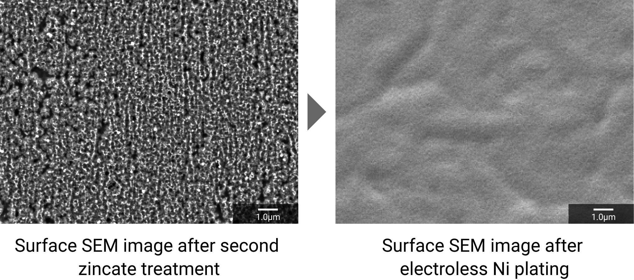
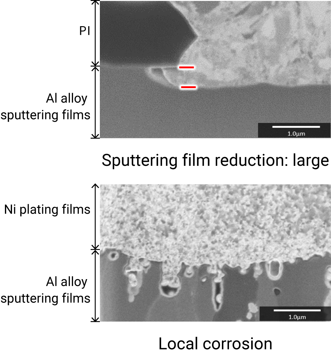
This electroless plating process for aluminum electrodes on wafers ensures no localized corrosion on aluminum electrodes and produces a uniform zinc oxide film, resulting in strong adhesion.
Uniform zinc oxide films on Al electrodes
TORYZA EL PROCESS
Conventional process
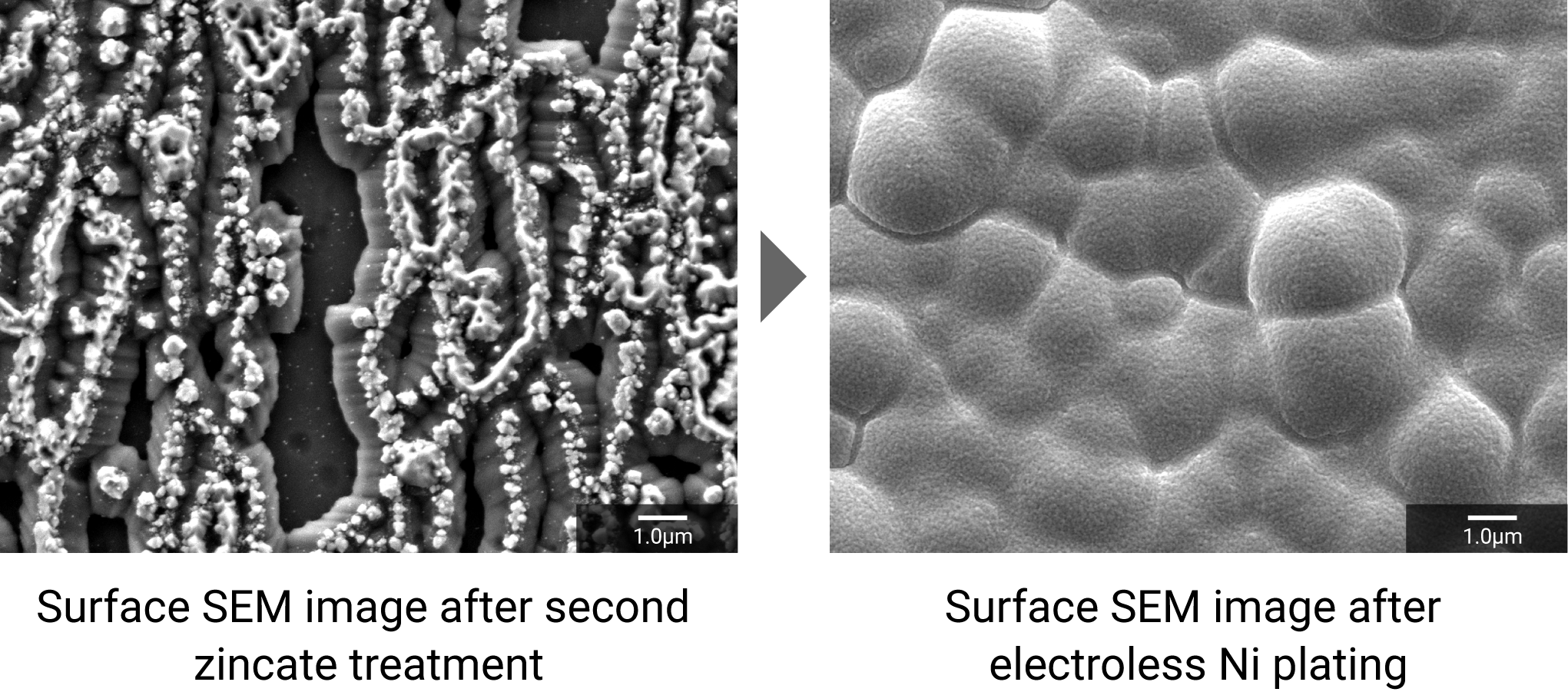
Reduce etching amount, prevent local corrosion of Al alloy sputtering films
TORYZA EL PROCESS
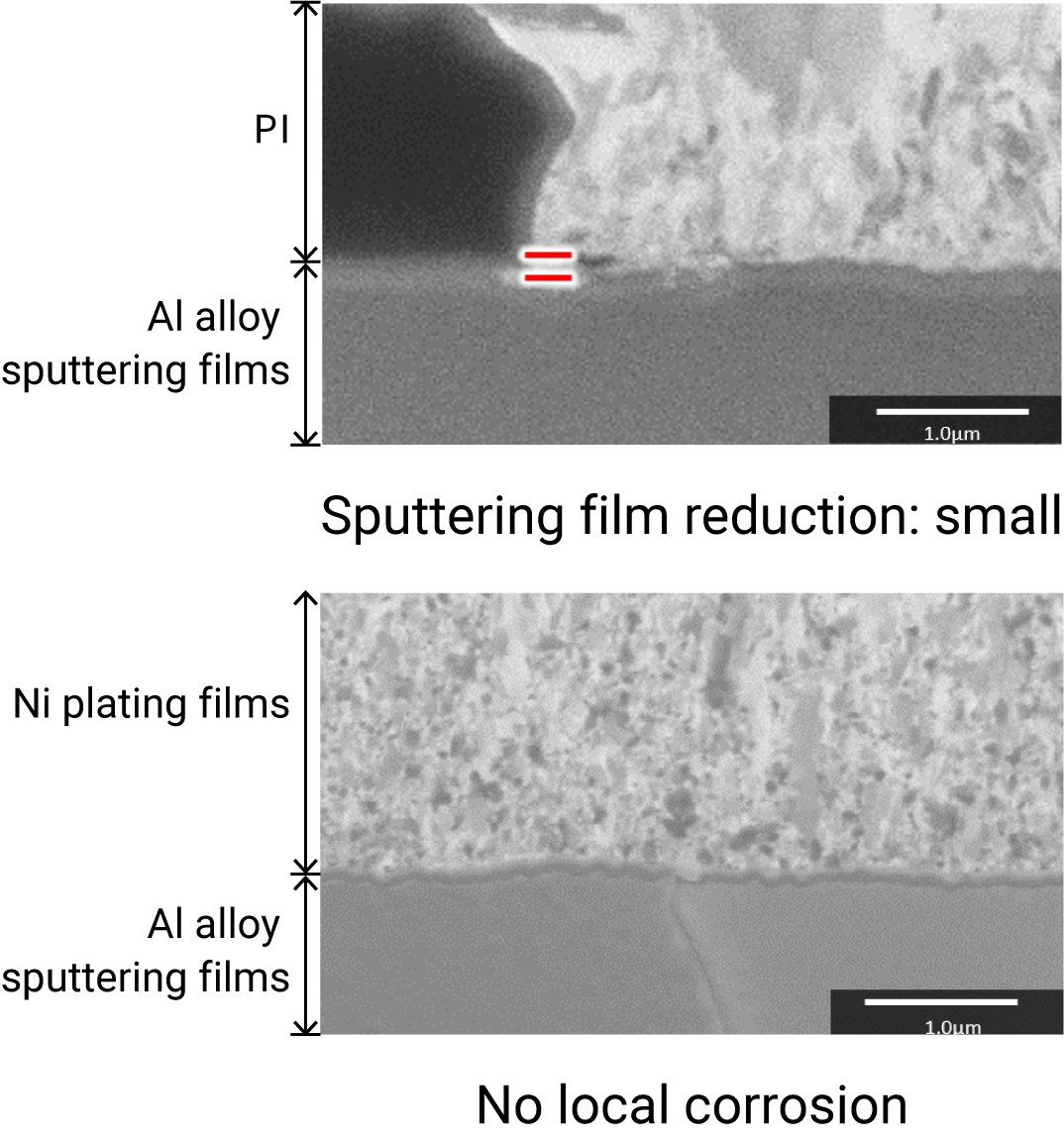
Conventional process
Electroless Ni plating films applicable to high temperature jointing
TORYZA NCR HRC

Conventional Ni plating film
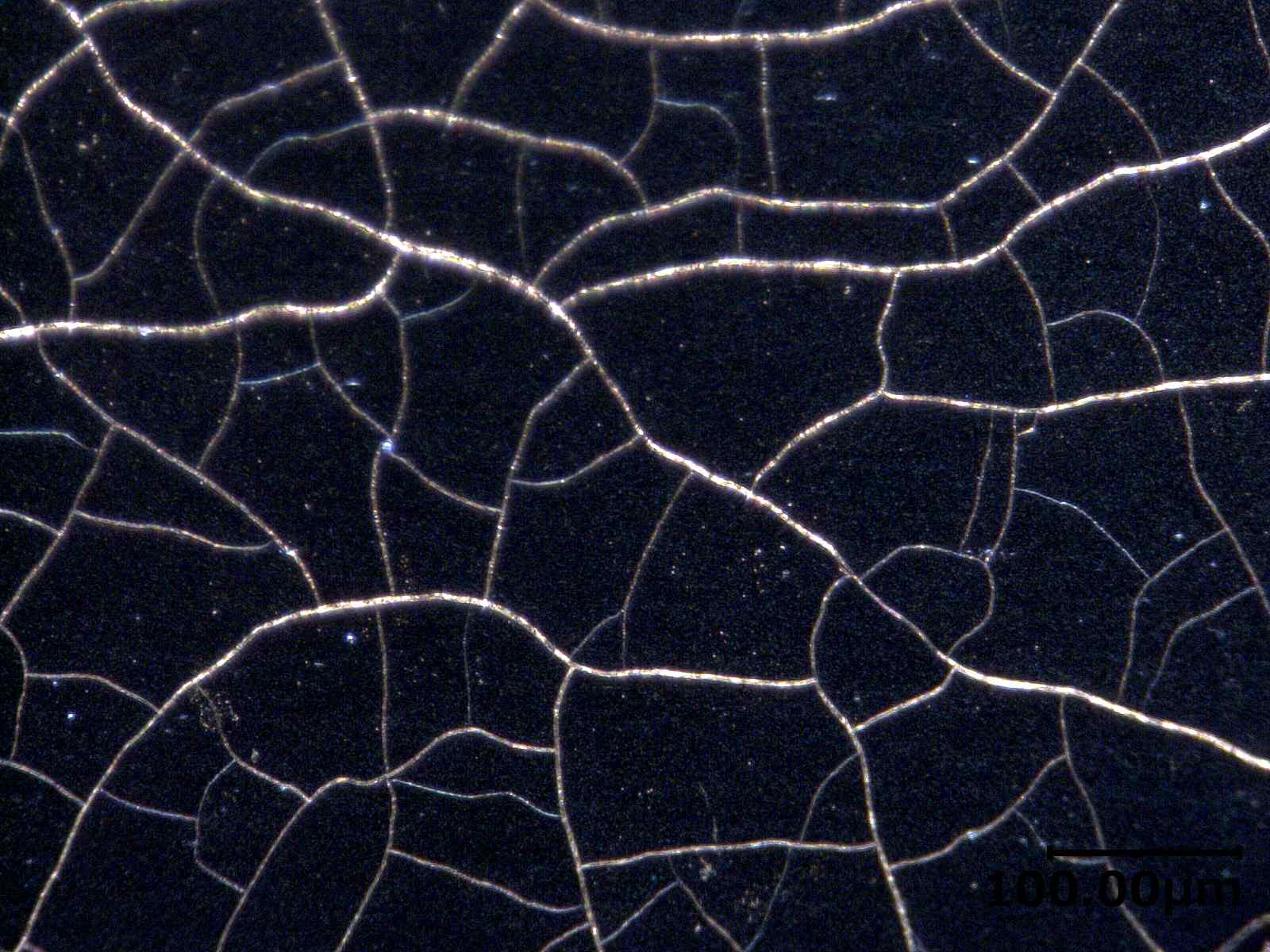
Heat treatment:400 ℃, 30 min
Indentation test by Erichsen tester (Ni thickness: 3 µm, indentation width: 0.5 mm)
Electroless Ni plating films applicable to high temperature condition
Crack occurrence of electroless Ni plating films after thermal-cycle and high-temperature test
| Electroless Ni plating films | Crack occurrence | ||
|---|---|---|---|
| After heat treatment | After thermal cycle | After high temperature test | |
| TORYZA NCR HRC | No | No | No |
| Conventional Ni plating film | No | Occur | Occur |
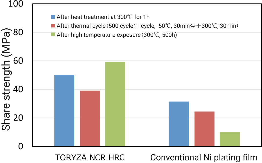
Presented by SANKEN, Osaka University Flexible 3D JISSO Collaborative Research Institute
SiC Chip:Ti sputtering on SiC chip, and form Ag sputtering layer
Jointing condition:Electroless Ni plating (7 μm thickness) on DBA substrate and sintering SiC chip on DBA substrate with Ag paste Adding 1MPa pressure, 300℃, 1h
Share strength after Ag sintering joint
Electroless plating system for wafer to make UBM
TORYZA EL SYSTEM
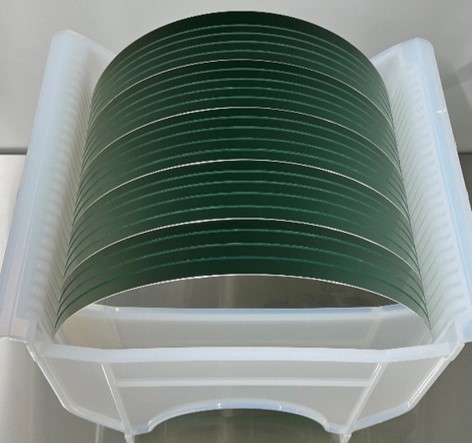
In the semiconductor industry, process certifications are commonly conducted using equipment developed by plating chemical suppliers. In response to this demand, we have developed TORYZA EL SYSTEM, an electroless plating system for semiconductor back-end processes that utilizes OKUNO's know-how gained from developing plating chemicals. TORYZA EL SYSTEM is equipped with cassettes on both sides that can respectively hold up to 25 pieces of 12-inch wafers. The carrier basket can handle 50 wafers simultaneously.
Large-scale system handling 50 wafers simultaneously
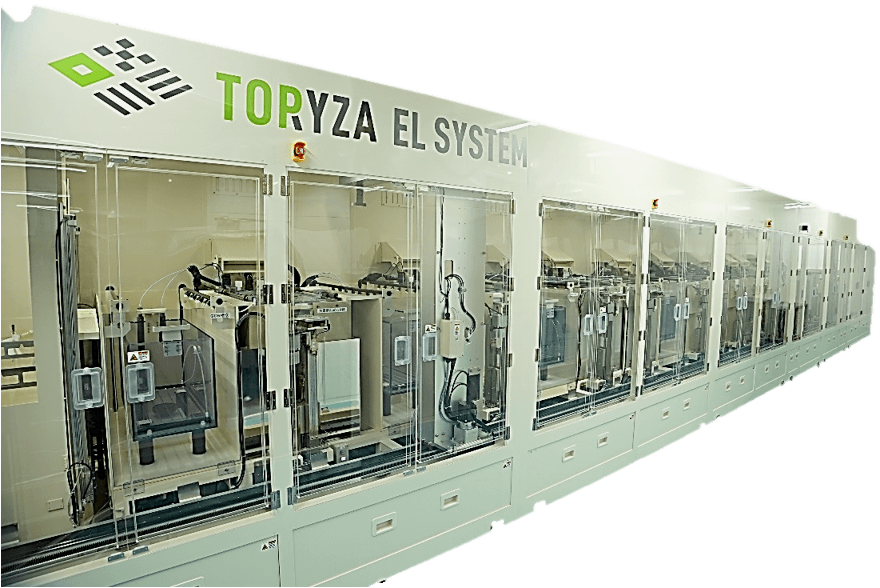
Overall view of TORYZA EL SYSTEM
- Applicable to 6 ,8, 12-inch wafer
- 25 pieces, full carrier, 2 lines
- Conform to ISO 14644-1 (Class 1000)
- Equipped with automatic recording system for production management and production monitoring
High thickness uniformity in same wafer piece
Wafer carrier
Thickness measurement slot
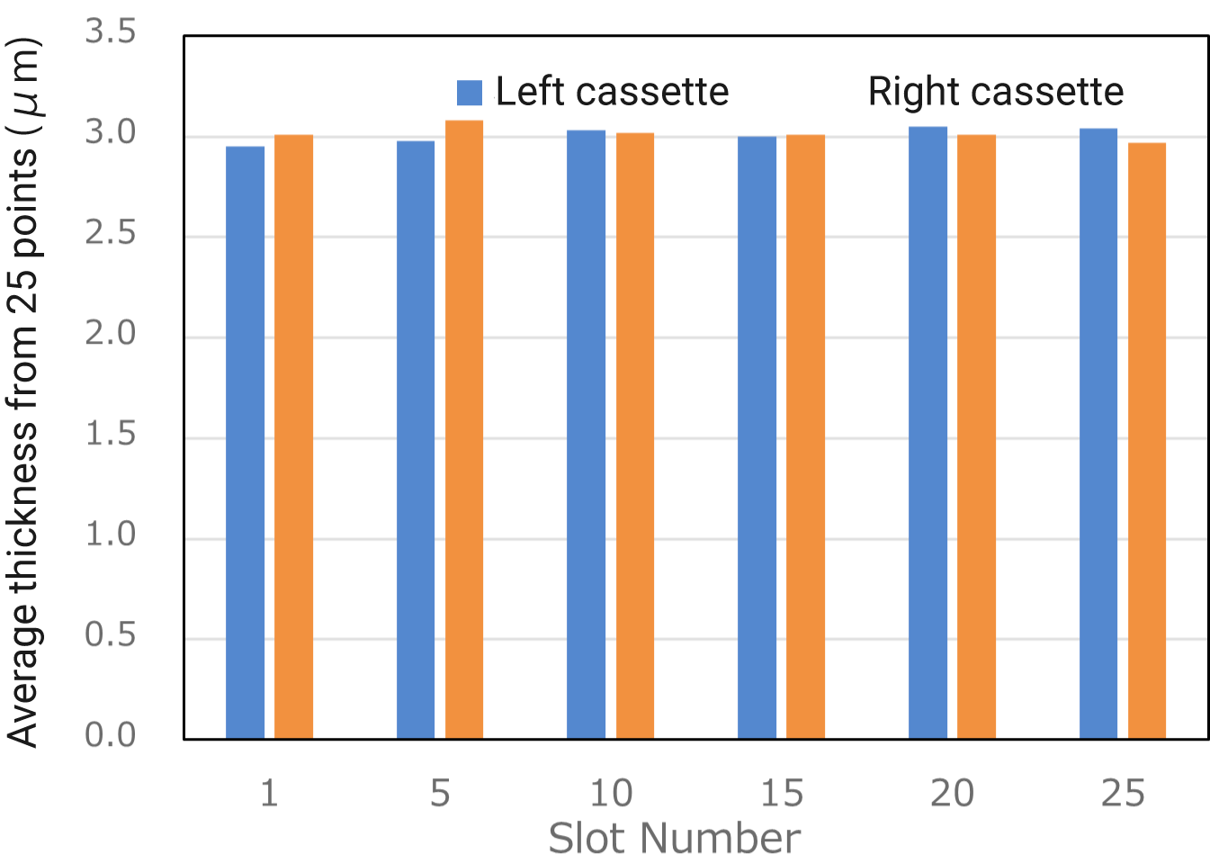
Thickness uniformity evaluation of electroless Ni plating in a 12 inch wafer