Acid copper plating additive for build-up PWBs with via and through holes
TOP LUCINA VT

Build-up wiring boards are used in the automotive industry for in-car navigation systems, as well as in telecommunications devices such as smartphones and tablets. They are called high-density interconnect (HDI) boards because of their high wiring density. Build-up wiring boards are manufactured by alternately laminating an insulating layer and a conductive layer on a substrate core with through-holes. Then, vias are formed on build-up layers by laser or other means for interconnection.
Stacked vias or pad-on vias on the build-up layers can significantly increase the pattern density of printed circuit boards, so via filling (filling vias by plating) has attracted attention. In addition, some components are inserted and mounted on the outermost layer of build-up substrates. Also, these substrates often have through-holes for internal connection from front to back, so advanced throwing power is highly demanded for an acid copper plating additive for via filling.
Therefore, we have developed a new additive for acid copper plating that satisfies both via filling performance and high throwing power in through holes.
Product features, specifications
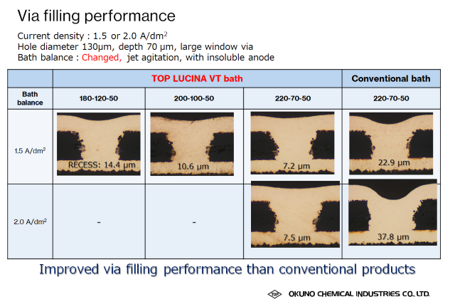
TOP LUCINA VT is the best additive for build-up PWBs with via and through holes. With general copper sulfate plating additives, it is necessary to increase the sulfuric acid concentration in the plating bath to ensure throwing power in the through-holes, Such high throwing bath compositions can’t fill vias sufficiently.
This product achieves excellent via filling plating performance and high throwing power in through holes. TOP LUCINA VT greatly contributes to the productivity improvement in the production lines of via and through-hole printed circuit boards. We offer a variety of products to support the surface treatment of printed circuit boards, so please feel free to contact us.

Acid copper plating additive for build-up PWBs with via and through holes
Okuno has developed a new additive, TOP LUCINA VT, for acid copper plating that satisfies both via filling performance and high throwing power in through holes. TOP LUCINA VT greatly contributes to the productivity improvement in the production lines of via and through-hole printed circuit boards. We offer a variety of products to support the surface treatment of printed circuit boards
