Featured
Additive for acid copper plating with high via-filling performance and thickness uniformity for fine patterns
TOP LUCINA NSV ADV

COVID-19 pandemic has drastically changed our lifestyles, and remote working and online business have become mainstream. The demands for telecommunication are sharply increasing, and high-class performance is required for the devices such as 5G smartphones, computers, data centers and car electronics. Thus, the technology for IC substrates is constantly making rapid progress.
To fabricate PWBs for telecommunication mobiles, build-up process has been widely used, and our copper electroplating additives have been globally adopted in the purpose.
Now, OKUNO has developed new additives for via filling by advancing stacked via technology to improve the degree of freedom of circuit wiring. This product can realize excellent film thickness uniformity for ultra-fine patterns suitable for high-speed transmission.
Product features, specifications
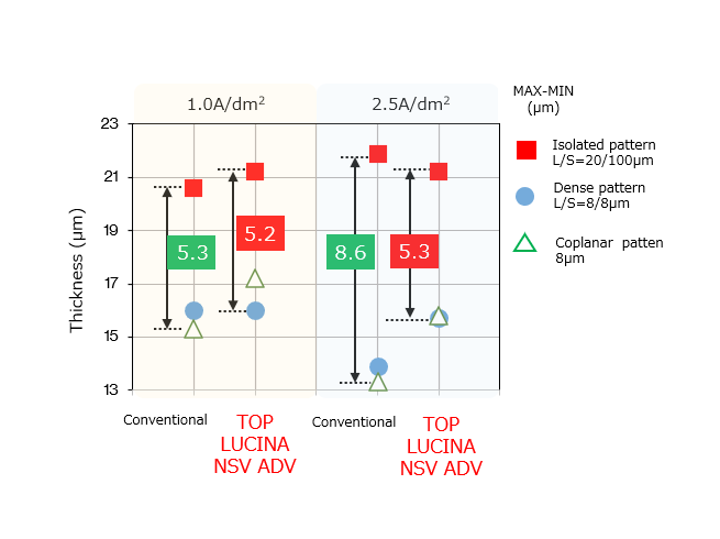
IC substrates have required the additives for via filling in copper electroplating. With conventional products, thickness variations have occurred if current densities increase to improve productivity.
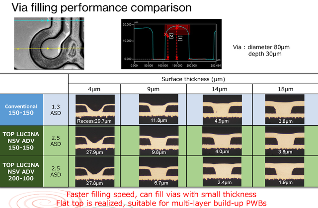
Our new product, TOP LUCINA NSV ADV achieves high film thickness uniformity in ultra-fine patterns while maintaining excellent via filling performance.
We have improved the polarization properties by optimizing the molecular structure of the inhibitor for enhanced via filling performance, This product is ideal for forming fine circuits for high-speed transmission, contributing to higher conductivity and reliability of electronic components and IC substrates.

Additive for acid copper plating with high via-filling performance and thickness uniformity for fine patterns
OKUNO has developed new additives for via filling by advancing stacked via technology to improve the degree of freedom of circuit wiring. This product can realize excellent film thickness uniformity for ultra-fine patterns suitable for high-speed transmission. Our new product, TOP LUCINA NSV ADV achieves high film thickness uniformity in ultra-fine patterns while maintaining excellent via filling performance.
